
When I got started in PCB design, layout seemed like the easy part. The CAD software enforces the schematics, so you just need to puzzle everything together until all connections are made. Right? At some point, you hit unexpected performance issues and decide to google around for solutions. Step by step you discover special ‘rules of thumb’, for example about decoupling capacitors or ground planes. This all seems very helpful and your designs improve steadily. But inevitably you will come across contradictions.
Unstable opamps, noisy signals, or even ‘magic’ issues that seem to ‘go away’ and come back later at random. Most designers will have experienced these kind of issues at some point. Often, these problems are caused by the layout.
There is a lot of contradicting advice to be found on the internet. Let’s say you have just learned to use ground planes, but then you read an application note from a big chip manufacturer suggesting split ground planes for their ADC. What is going on? Have you been doing it wrong all this time? Surely the appnote from a big chip company cannot be wrong?
One source of this problem is that electronics components have changed a lot over the last decades. Low-frequency design (think audio range) will result in different design rules than modern high-speed design. A lot of the ‘old’ design rules (that used to work fine decades ago) keep circulating on the internet, but in most cases are no longer applicable.
Nowadays, even if you think you are doing low-frequency stuff, you most likely still have some high-frequency signals on your board. The key thing here is the rise time of signals. Modern digital chips have rise times that can be even faster than 1 ns.

This means every switching digital signal has high-frequency contents (up into the GHz range!). Even if you’re only toggling a LED pin at 5Hz from a cheap microcontroller, you still have frequencies of hundreds of MHz running across your board.
These fast edge rates have the side effect of taking quick gulps of current from the power rail, which leads to short voltage dips inside digital chips. These voltage dips in the power rail can couple into other I/O signals and spread across your board. This means that even a non-switchig GPIO may contain high-frequency contents!
You must take high-frequency design into account to avoid unwanted side-effects. A good layout will greatly improve EMC performance and product reliability.
In a two-layer layout, try to dedicate the bottom layer to GND. Try to route all signals on the top layer, only use the bottom layer if you really have to. If there is no way to make this work, consider going to a four-layer board. Yes, they are a bit more expensive, but is it worth the extra respin if you fail EMC testing?
For a four-layer board, definitely dedicate one layer to GND only. The ground plane should cover the whole board and must not contain any other signals. Do not create any splits or holes in the GND plane. Watch out for large groups of via’s: they can accidentally cut big holes in the GND plane! Don’t bother with a power plane, unless you have specific requirements (e.g. high-current low-voltage FPGA chips) Just route the power rails as wide tracks.
These are some basic tips for a good layout. You may already know some of them. But what are they based on? Why use a ground plane?
The answer is return current. In electronics design, we are used to just think about voltages: a 3.3v signal needs to go from A to B. But this omits the basic working principle of electronics: current flows in loops. A signal does not just go from chip A to chip B. What happens after chip B? The current goes through the chip (or decoupling capacitor), through the GND plane, back into chip A. The ground plane is a tool that helps ensure there is always an optimal path for the return current. If you have no GND plane (or a track is routed over a split in the GND plane), the return current needs to take a detour. As we’ll see later, you really don’t want that.
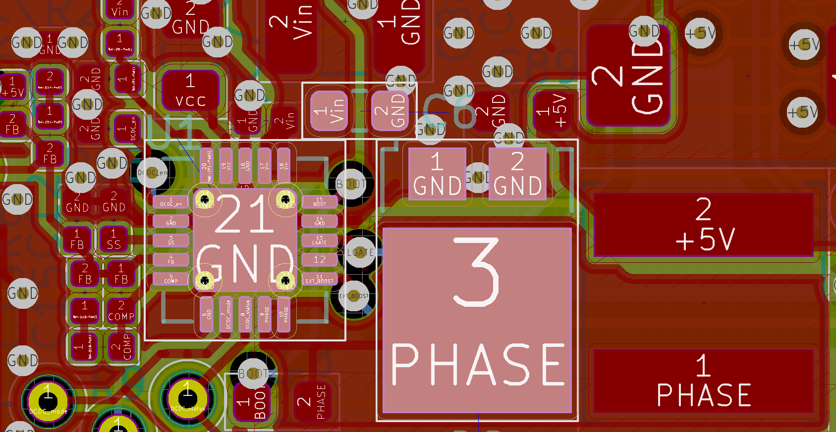
Some parts need extra attention due to their high-frequency contents. High-speed interfaces (clock lines, USB, DDR, etc) will have very fast edge rates that can cause problems even if you route them above a GND plane. Another example is DC/DC controllers. While they switch at a moderate frequency (100kHz up to to a few MHz), they too have very fast edge rates. Their fast edge rates and high power make them a good source of EMC issues, requiring careful layout. As an example, let’s take a DC/DC buck converter. A buck converter is basically a fast high-power switch (high dV/dt edges) to take quick pulses of current (high dI/dt) and smooth them via an LC-filter into an output voltage. Let’s compare two layouts: layout A and layout B. Which one is better? Why?


Let’s look at the high-frequency part of the input current. Remember, we’re not interested in DC, but the nasty high-frequency effects. Look at the connection between C9 and U1. The AC-current loop will travel ‘through’ C9 and needs to find a path back to U1. How? It needs to take a big detour. For layout B the GND pads of U1 and C9 are right next to each other: much better!
The AC-current loop for layout A is clearly much bigger than for B. Why is this a problem? A big loop with high-frequency current is a crude magnetic coil acting as a loop antenna! The larger this loop, the more power this antenna will emit. This can disturb sensitive signals on your PCB and interfere with other electronics nearby. This means a high chance of failing to meet mandatory EMC compliance standards and reduced product performance.
As you may have noticed, the recurring theme here is keeping current loops small. Or more specific: the area enclosed by the current loop should be small.
This is the key to a reliable, high-performance layout: don’t think in voltage signals, but in current loops. Almost all other design rules can be derived from this principle. Why use a ground plane? It helps define small current loops (return current right under the trace!). Why place decoupling capacitors near the IC? It keeps the current loop small.
Almost all rules of thumb can be tested against the principle of current loops. A split ground plane with a trace running over the split? Large current loop, bad idea. Even fancy datasheets or application notes sometimes get this wrong!
Hopefully, these tips help you design a rock-solid circuit board. If you have questions about this topic, don’t hesitate to contact me at pcbdesign@jitter.company.
Want to feel confident that your board will work right the first time? Curious if there is room for improvement? Have a look at our PCB design check service!


